♪
♫
♩
Board & Component Specifications
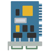
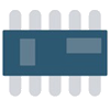
The product is an industrial main control board. The PCB is a 10+ layer HDI board, with components including large BGA and QFN. The surface finish is ENIG — this is to keep the pads flat, which helps BGA soldering.
Quality Assurance
We provide X‑ray inspection to ensure soldering quality.
Impedance and signal control are achieved through a matched lamination structure. The VIA holes in the BGA area go through resin plugging, plating, and polishing — all to make sure the BGA balls are soldered properly.
Manufacturing Standards
Even for sample quantities, we use fully automatic pick‑and‑place machines. No compromise on quality.
We decide whether to use step stencils based on the pad conditions across the entire board — to ensure proper solder paste thickness and soldering quality.
For IC supply, we purchase from authorized distributors. Genuine parts only.
For this type of main control PCBA, we manufacture exactly to the customer's requirements.
Try Our Capability
We can also solder one BGA and one QFN for you — on a chargeable basis — so you can test our manufacturing capability. The sample cost will be based on the quote. Rest assured, soldering just one BGA and one QFN will not be expensive.
If you confirm cooperation with us, this sample cost will be deducted from your future order. That means we are essentially sampling for you — for free.