|
| Fabriaction flow |
PCB layers |
1-2 L |
| Lamination Cutting |
PCB thickness |
0.4 mm , 0.6 mm , 0.8mm , 1.2 mm , 1.6 mm , ≥2.0 mm |
| PCB lamination |
Fr4 TG 130℃/150℃/170℃/180℃ 、 High-Speed Isola, Rogers , |
| Mech Drill |
Holes type |
Trough holes |
| Smallest hole size |
≥0.15 mm |
| Hole distance |
36 mil |
| Rout for metal edge |
|
|
| Hole Plating & Edge plating |
Thickness of hole wall |
20 um |
| Circuit |
Copper weight |
Outer copper 1 oz 、≥2 oz |
| Line width |
3 mil |
| Line space |
3 mil |
| Hole ring |
6 mil |
| Half-plating holes |
Hole size |
0.5 mm min |
| Solder mask |
Solder mask openning |
≥1.5mil |
| Via holes |
Tented with solder mask 、solder mask openning 、plug via holes |
| Solder mask thickness |
15±10μm |
| Surface treatment |
Surface treatment |
Lead-free hasl 、OSP 、ENIG 、Immersion Silver |
| Gold thickness @ ENIG |
1-≥3 u'' |
| Silkscreen text |
Silkscreen Line Width |
6 mil |
| Rout shape |
Inner cutout : |
24 mil |
| V-cut : |
Across , Jumper |
| V-cut degree : |
30° 45 ° 60° |
| PCB shape |
Regular and irregular |
| PCB Size |
≤ 200 cm |
| Bevel edge |
20°、 30 °、45 ° |
| Quality |
Tolerance : |
|
| Pth / npth Hole size |
+/- 3 mil 、 +/- 2 mil |
| Board thickness |
T≥1.0mm +/- 10% ; T<1.0mm +/- 0.1 |
| Line width |
+/- 20% |
| Outline |
±0.15mm |
| IPC |
class II , class III 、IPC-6018A |
| Testing |
4 wires low impedance testing , electronics testing , flying probe , AOI |
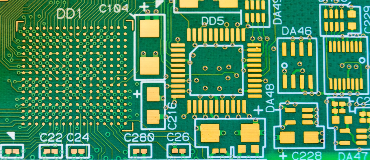 |
| Fabriaction flow |
PCB layers |
≥4L |
| Lamination Cutting |
PCB thickness |
0.4 mm , 0.6 mm , 0.8mm , 1.2 mm , 1.6 mm , ≥2.0 mm |
| PCB lamination |
FR4 TG 130℃/150℃/170℃/180℃ 、CTI ≥175V 、UL-94 V0 |
| Inner layers |
Inner layer |
copper weight H oz , ≥1 oz |
| Layer stackup |
PP type 7628 , 1080, 2116 , customized upon impedance control |
| Laser Drill ( Buried 、blind hole ) |
Smallest hole size |
≥0.1mm |
| Mech Drill |
Holes type |
Trough holes & Micro-via |
| Smallest hole size |
Mech Drill ≥0.15 mm |
| Hole distance |
36 mil |
| Rout for metal edge |
|
|
| Hole Plating & Edge plating |
Thickness of hole wall |
20 um 、25 um |
| Circuit |
Copper weight |
Outer copper 1 oz , ≥2 oz |
| Line width |
3 mil |
| Line space |
3 mil |
| Hole ring |
6 mil |
| BGA size |
≥10mil @ hasl 、≥8mil @ ENIG |
| Distance between center |
≥0.45mm |
| Impedance |
Tolerance upon value |
Value>50Ω , ±10% 、≤50Ω ±5Ω |
| Single line |
≤75Ω |
| Difference line |
≤150Ω |
| Solder mask |
Solder mask openning |
≥1.5mil |
| Via holes |
Tented with solder mask 、solder mask openning 、plug via holes |
| Solder mask thickness |
15±10μm |
| Surface treatment |
Surface treatment |
Lead-free hasl 、OSP 、ENIG 、Immersion Silver |
| Gold thickness @ ENIG |
1-≥3 u'' |
| Silkscreen text |
Silkscreen Line Width |
6 mil |
| Rout shape |
Inner cutout : |
24 mil |
| V-cut : |
Across , Jumper |
| V-cut degree : |
30° 45 ° 60° |
| PCB shape |
Regular and irregular |
| PCB Size |
≤ 200 cm |
| Bevel edge |
20°、 30 °、45 ° |
| Quality |
Tolerance : |
|
| Pth / npth Hole size |
+/- 3 mil 、 +/- 2 mil |
| Board thickness |
T≥1.6mm +/- 10% ; T<1.6mm +/- 0.1 |
| Line width |
+/- 20% |
| Outline |
±0.15mm 、±0.1mm |
| IPC |
class II , class III 、IPC-6018A |
| Testing |
4 wires low impedance testing , electronics testing , flying probe, AOI |
| The PCBs are fabricated according to IPC 6012 class II 、PCBs are designed according to IPC -2221 , IPC -2222 , class II |
|
|